 NTNU NanoLab
 UiO MiNaLab
 USN MST-Lab
 SINTEF MiNaLab
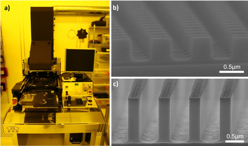
UV-Nanoimprint Lithography EVG 620 Smart NIL aligner
Model: EVG 620 Smart NIL aligner
Manufacturer: EVG
Area: Clean room

UV-Nanoimprint lithography: High throughput, large area nanopatterning with excellent resolution and repeatability.
At SINTEF MiNaLab, nanoimprint lithography (NIL) based on EVG60 NT is employed for high throughput, large area nanopatterning on 6 inch wafers with excellent resolution (sub 100nm) and repeatability. Application examples include:
- Diffractive Optical Elements (DOE): Binary and 4-level gratings.
- Metasurfaces: Nanomaterials 13.3 (2023): 436.
- Nanostructures for Surface Enhanced Raman Spectroscopy (SERS): Nanomaterials 13.10 (2023): 1598.
UV-NIL Processing:
The process involves transferring patterns from a master template wafer (prepared using techniques like electron beam lithography, i.e. EBL), to sample wafers via imprinting using a stamp and subsequent Reactive-Ion Etching. A stamp/mold is prepared by coating the master wafer with a photo (UV) sensitive liquid stamp material. Exposure to UV light hardens the stamp material, creating the mold. In the next step, a sample wafer is coated with a UV curable liquid resist (mr-NIL210-200nm) and is pressed against the mold that contains the patterns from the master wafer. The UV light exposure solidifies the liquid resist, transferring the patterns from the mold onto the thin layer of resist coated over the sample wafer. The patterns on the resist layer are then etched onto the sample wafer using Reactive Ion Etching.
