 NTNU NanoLab
 UiO MiNaLab
 USN MST-Lab
 SINTEF MiNaLab
Suss Mask Aligner MA150e
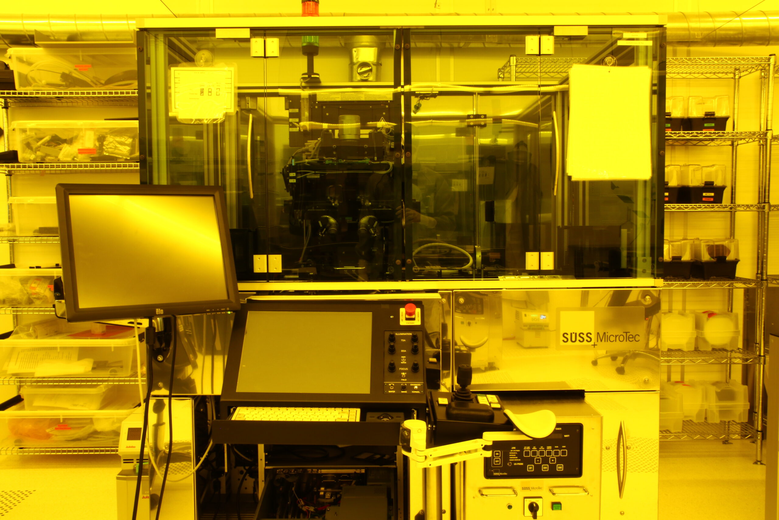
Model: MA150e
Manufacturer: Suss MicroTec
Area: Clean room

Wafer size: 150 mm
The light source on this exposure tool is a 1000W Hg lamp, used with I-line filter (365nm) for the UV exposure of different resist types. The tool is either used in proximity exposure mode or soft-contact mode. The typical resolution that can be obtained is about 4 µm in proximity mode and 2 µm in soft-contact mode. Both top-side alignment (TSA) and back-side alignment (BSA) are available. The tool has fully automated cassette-to-cassette wafer handling.
A photomask with a certain structure is aligned with the wafer in very close proximity. During exposure, the shadow cast by the mask structure is transferred to the wafer. The resulting exposure quality depends on both the precision with which the mask and wafer are spaced apart and the optical system used for exposure.
Where lithographic processes require the alignment of structures on only one side of the device wafer, top-side alignment is used to align the fiducials on the mask with those of the wafer.
For double-sided applications, the alignment of the structuring on the wafer back side with the structures on the front is required. Optical bottom side alignment is normally used for this type of alignment. An integrated camera system detects the mask structures and the structures on the wafer back side and aligns them with each other. The wafer position is determined and stored prior to loading, since the wafer afterwards conceals the mask target.
