 NTNU NanoLab
 UiO MiNaLab
 USN MST-Lab
 SINTEF MiNaLab
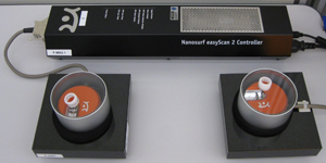
STM 1, Nanosurf
Contact:

Verner Håkonsen
Senior Engineer
NTNU NanoLabResponsible for Characterization at NTNU NanoLab. Tool-responsible on SEM/STEM, FIB, AFM, profilometers, wire bonder and coaters for SEM prep. Has also experience in chemical methods, such as nanoparticles synthesis.
+47 92057253
verner.hakonsen@ntnu.no
Model: easyScan 2
Manufacturer: Nanosurf
Area: Chemical area
The Nanosurf Scanning Tunneling Microscope is an easy to use instrument with which you can achieve down to atomic resolution of the surface of conducting samples, in air. It is a probe microscope that measures tunneling currents between the sample and the tip. It is mainly used with clean Au and graphite samples in student labs.
Sample Specification:
Only conducting samples. Maximum sample diameter 10 mm, but no limitations in thickness. The maximum scan range of this STM is 500 nm, and 200 nm in Z-direction.
