NTNU NanoLab
 UiO MiNaLab
 USN MST-Lab
 SINTEF MiNaLab
Dielectric Etch – SPTS Synapse
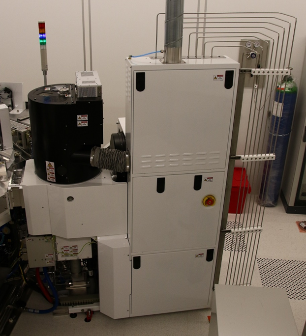
Model: SPTS Synapse
Manufacturer: SPTS Technologies Ltd
Area: Cleanroom

Tool description
A stand-alone, single wafer etcher with one reactor and cassette to cassette automatic wafer handling. The process module uses a high-density plasma source and is designed to etch strongly bonded materials. The process chamber is heated to 130°C to reduce the amount of by-product deposition and improve MTBC. The chamber is also surrounded by permanent magnets which result in a higher plasma density than conventional ICPs (by a factor of ~10x). Higher plasma density means higher etch rate of strongly bonded materials and the capability of running at reduced pressure. The latter extends mean free paths and leads to better directionality and less by-product ‘fencing’.
Technical information
- Materials allowed: 150 mm Si substrates, with thin films of SiO2, Si3N4, Al, polySi and photoresist.
- Substrate thickness range: Minimum 300 µm, Maximum 2 mm.
- Substrate clamping type: Electrostatic.
- Optional wafer edge protection: Non-contact wafer edge protection (WEP) rings with either 4 mm or 2 mm wafer edge overlap can be used with wafers up to 1mm thick.
- Wafer edge exclusion zone: 8 mm without WEP, 10 mm with WEP.
- Plasma source: ICP type, High frequency RF generator (13.56 MHz) with 2.2kW maximum usable power.
- Substrate bias: High frequency RF generator (13.56 MHz) with 1.2 kW maximum usable power. Pulsing of bias power is possible.
- Process gases available: C4F8 , CF4 , SF6 , O2 , H2 , He, Ar
- Process pressure: Up to 50 mTorr
- Substrate holder temperature range: -10 °C to +40 °C
Contact persons
Process responsible: Anand Summanwar
Senior Process Scientist
Dept. of Smart Sensors & Microsystems
SINTEF Digital
Email: Anand.Summanwar@sintef.no
Tel: +47 9823 0490

Service responsible: Tri Huu Nguyen
Senior Engineer
Dept. of Smart Sensors & Microsystems
SINTEF Digital
Email: TriHuu.Nguyen@sintef.no
Tel: +47 9162 2832