NTNU NanoLab
 UiO MiNaLab
 USN MST-Lab
 SINTEF MiNaLab
Deep Silicon etch / DRIE – SPTS DSi
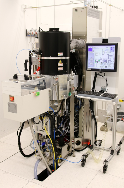
Model: SPTS DSi
Manufacturer: SPTS Technologies Ltd
Area: Clean room

Tool description
A stand-alone, single wafer etcher with one reactor and a manual wafer loading system through a single wafer load-lock. The reactor has a decoupled, high-density inductively coupled plasma (ICP) source. It is purpose built for deep reactive ion etching (DRIE) and high aspect ratio etching of silicon using the Bosch (switched) process. In addition, it is also possible to perform (continuous) RIE etch processes such as etching of thin films of SiO2, Si3N4, polySi and organic materials.
Technical information
- Materials allowed: 150 mm Si substrates, with thin films of SiO2, Si3N4, Al, polySi and photoresist. On this tool we also allow wafers with Au, Pt and PZT, if these materials are not exposed to the plasma.
- Substrate thickness range: Minimum 300 µm, Maximum 2 mm.
- Substrate clamping type: Electrostatic.
- Optional wafer edge protection: Non-contact wafer edge protection (WEP) ring with 4.5 mm wafer edge overlap can be used with wafers up to 1mm thick.
- Wafer edge exclusion zone: 8 mm without WEP, 10 mm with WEP.
- Plasma source: ICP type, High frequency RF generator (13.56 MHz) with 3kW maximum usable power.
- Substrate bias options: High frequency RF generator (13.56 MHz) with 1.5 kW maximum usable power or Low frequency RF generator (375 kHz) with 300 W maximum usable power. Pulsing of bias power is possible for both.
- Process gases available: SF6 , C4F8 , O2 , Ar , CF4
- Process pressure: Up to 20 Pa
- Substrate holder temperature range: -10 °C to +40 °C
Contact persons
Process responsible: Anand Summanwar
Senior Process Scientist
Dept. of Smart Sensors & Microsystems
SINTEF Digital
Email: Anand.Summanwar@sintef.no
Tel: +47 9823 0490

Service responsible: Tri Huu Nguyen
Senior Engineer
Dept. of Smart Sensors & Microsystems
SINTEF Digital
Email: TriHuu.Nguyen@sintef.no
Tel: +47 9162 2832