 NTNU NanoLab
 UiO MiNaLab
 USN MST-Lab
 SINTEF MiNaLab
Wafer Bonding System EVG 501
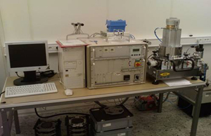
Model: EVG501
Manufacturer: Electronic Visions Group (EVG)
Area: G2-33 Cleanroom

The EVG501 Wafer Bonding System is a highly flexible R&D system that can handle small substrate pieces up to 100 mm wafers. The tool supports a variety of bonding processes, such as anodic, glass frit, eutectic, diffusion, fusion, solder,and adhesive bonds, as well as other thermal processes, including oxide removal and high temperature bakes under a controlled atmosphere. The system also offers quick re-tooling with a conversion time of less than five minutes, making it ideal for universities and R&D as well as small-volume production applications.Available bonding processes at HiVe:Anodisk: e.g. Silicon to Glass, Fusion: Silicon to Silicon and SLID: Au-Sn, Cu-Sn.
Technical Data: Substrate thickness range: 200µm – 2,000µm
Clamping ring exclusion zone: 2mm / 4mm (100mm wafers)
Bonding temperature ramp: computer-controlled program
Bonding Temperature: room temperature to 550ºC
Bonding force: 7 kN
Vacuum: 10-3 Torr
Voltage: 0 – 2000 V
Bonding temperature ramp: computer-controlled program
Bonding Temperature: room temperature to 550ºC
Bonding force: 7 kN
Vacuum: 10-3 Torr
Voltage: 0 – 2000 V
