 NTNU NanoLab
 UiO MiNaLab
 USN MST-Lab
 SINTEF MiNaLab
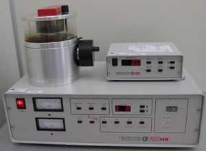
Sputter Coater for SEM Sample Prep.
Contact:

Verner Håkonsen
Senior Engineer
NTNU NanoLabResponsible for Characterization at NTNU NanoLab. Tool-responsible on SEM/STEM, FIB, AFM, profilometers, wire bonder and coaters for SEM prep. Has also experience in chemical methods, such as nanoparticles synthesis.
+47 92057253
verner.hakonsen@ntnu.no
Model: 208 HR B
Manufacturer: Cressington
Area: Characterisation

This sputter coater is used to produce extremely thin conducting layers on non-conducting samples, which eliminate charging and improve contrast on low density materials. Depending on the material chosen, grain-free uniform coatings can be achieved. Coating thickness is controlled by a thickness controller, and the resolution is better than 0.1 nm. The instrument is designed for coating thicknesses between 1 nm up to 20 nm, but can be used for thicker films as well.The materials available at NanoLab are
- Pt/Pd (80/20)
- Au/Pd (80/20)
- Au/Pd (60/40)
- Ta
- W
- Pt
- Au
Sample Specifications:
This sputter coater is intended for SEM sample preparation only. 5” wafers are the maximum size that will fit in the chamber. FIB stubs can easily be inserted in the holes on the chuck.
