 NTNU NanoLab
 UiO MiNaLab
 USN MST-Lab
 SINTEF MiNaLab
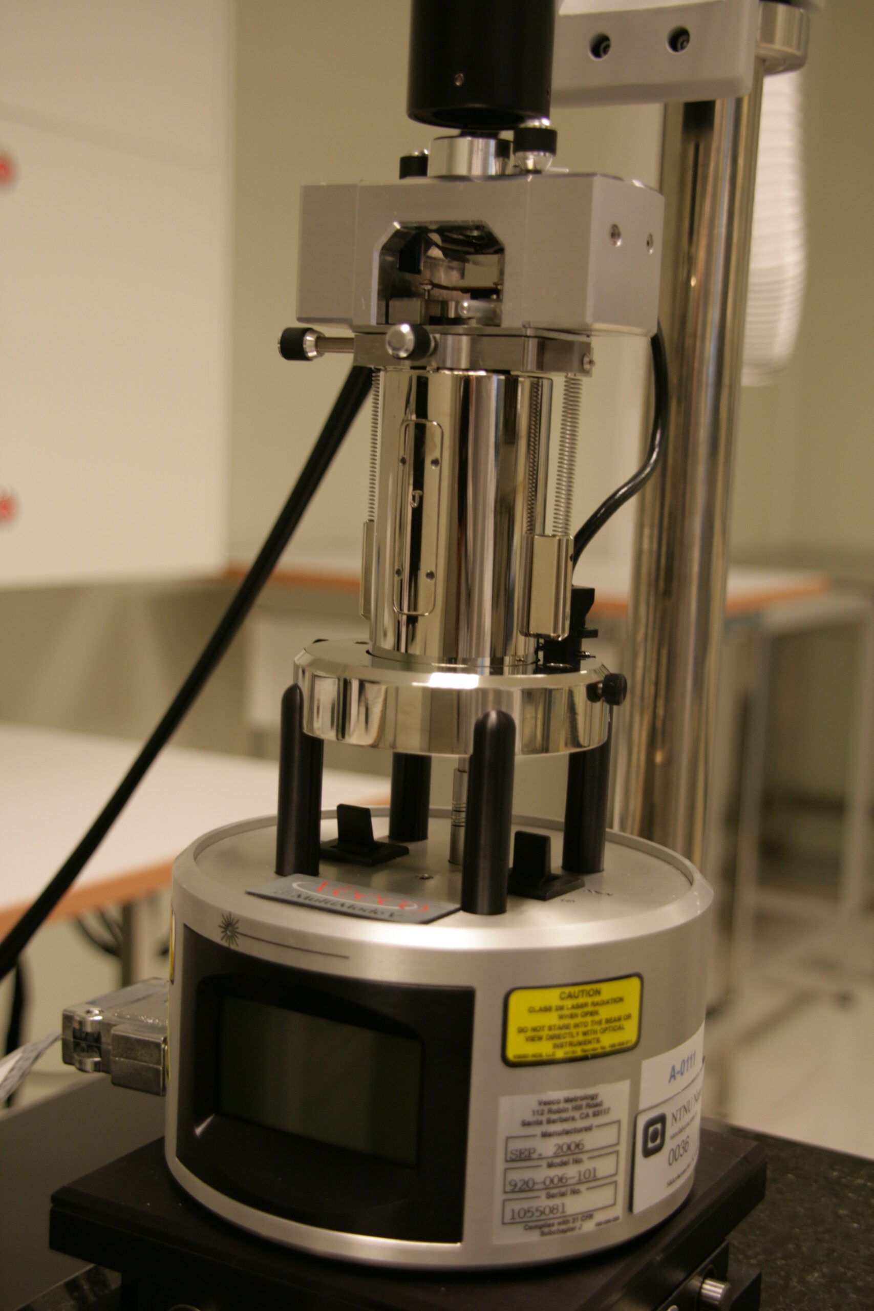
AFM, Veeco
Contact:

Verner Håkonsen
Senior Engineer
NTNU NanoLabResponsible for Characterization at NTNU NanoLab. Tool-responsible on SEM/STEM, FIB, AFM, profilometers, wire bonder and coaters for SEM prep. Has also experience in chemical methods, such as nanoparticles synthesis.
+47 92057253
verner.hakonsen@ntnu.no
Model: diMultimode V
Manufacturer: Veeco Metrology
Area: Characterisation
Atomic Force Microscopy offers topographic measurements of surfaces with accuracy in the nanometric scale. It is a useful tool for studying surfaces of various materials systems, including both organic and inorganic materials. The instrument can be used in contact and tapping mode, and can also map lateral forces. ScanAsyst is a third possible mode, which uses peak force mode to calculate the optimal settings for every individual sample. It is a new technique, which makes AFM imaging available also to inexperienced users.
Topography, roughness, softness are examples of what sample properties the AFM can give information about.It is possible to perform measurements in the temperature range of -35°C to 250°C in air or inert gas.
The AFM can in addition offer studies of soft materials, including the use of a liquid-cell. The liquid cell can be filled with water, buffer, oil or other liquids. It is also possible to coat the tip making it sensitive to different active sites on the surface (demands user knowledge on functionalization of the tip). Force spectroscopy is an option to make force-distance curves. Nanoindentation is not possible with the probes we have, but diamond tips for indentation can be bought and used buy researchers who have an interest in this. The software permits, among other things, roughness and distance calculations, 3-D and 2-D presentations, multi scanning and 8 simultaneous scan- views for detailed investigations of specific areas of the sample.
Sample Specifications:
This AFM is designed for samples up to 15mm in diameter having a maximum thickness of 6mm. The samples must be attached to magnetic sampleholders, which are available in the cleanroom. The scanning area is maximum 160 µm. The AFM can be used on most materials that are not too rough. To study particles, these have to be firmly attached to the surface.
